

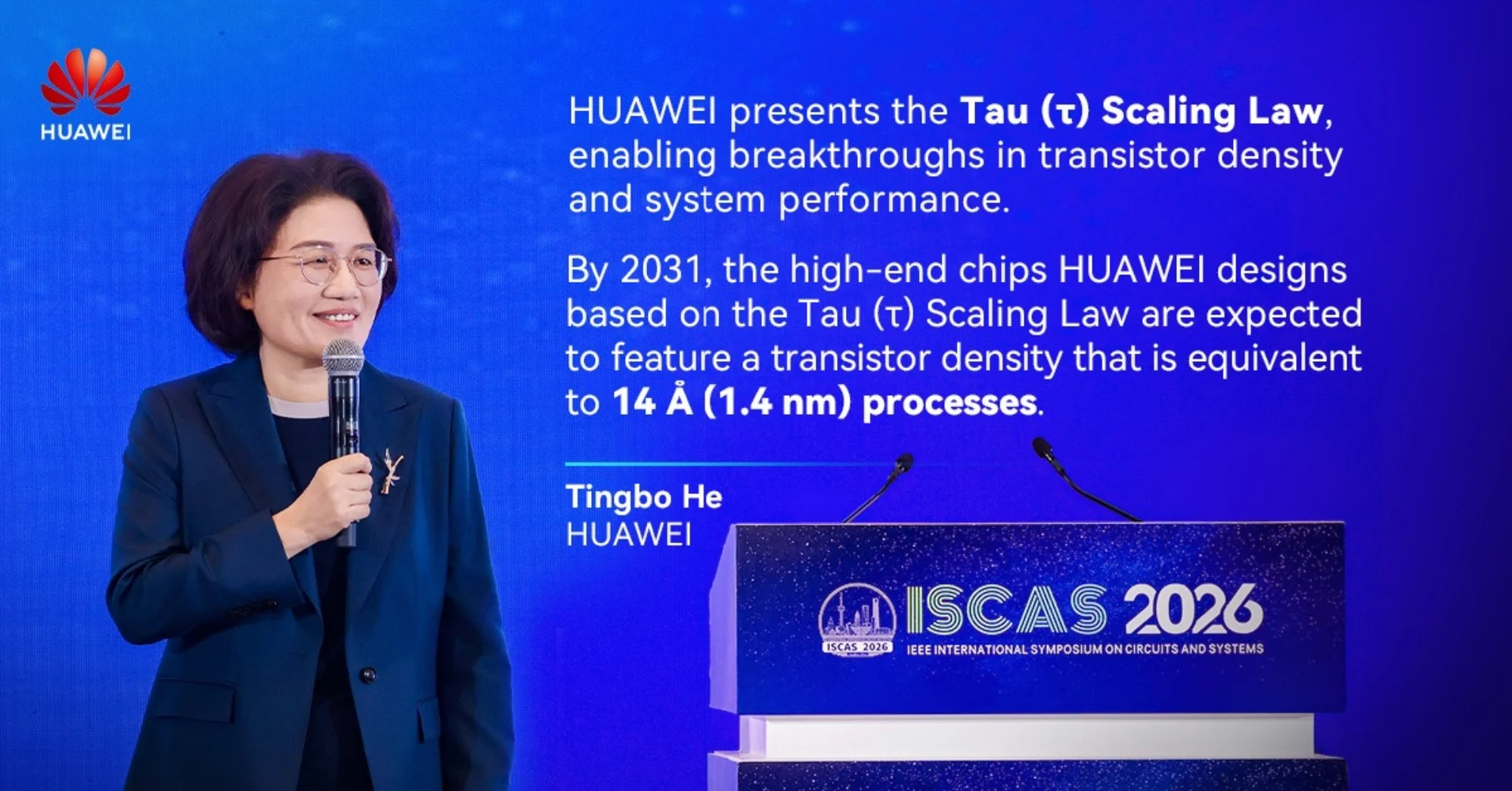
Chinese tech giant Huawei has unveiled what it describes as a new semiconductor development principle called the “Tau Scaling Law”, which the company claims could eventually allow its future chips to achieve transistor density equivalent to 1.4nm-class processes by 2031. The announcement was made during the 2026 IEEE International Symposium on Circuits and Systems (ISCAS) in Shanghai by He Tingbo, president of Huawei’s semiconductor business and director of its Scientist Committee.
According to the company, the Tau Scaling Law proposes a shift away from the industry’s traditional dependence on transistor miniaturisation, commonly associated with Moore’s Law. Instead, Huawei says the new approach focuses on reducing the time it takes for signals and data to move through chips and computing systems, with the aim of improving performance, efficiency, and transistor density through architectural and system-level optimisations.
A Different Approach To Chip Scaling
Huawei’s presentation comes at a time when China continues to face US export restrictions on advanced semiconductor equipment, particularly extreme ultraviolet (EUV) lithography systems used for cutting-edge chip production. Analysts have generally viewed these sanctions as one of the biggest barriers preventing Chinese firms from matching the world’s most advanced semiconductor manufacturing processes through conventional scaling methods.
To recap, Huawei was placed on the US Entity List in 2019, cutting the company off from many American technologies and severely affecting its smartphone and semiconductor operations. Despite this, the company staged a notable comeback in 2023 with the launch of its 5G-capable Mate 60 series smartphones, powered by a 7nm chip reportedly produced by China’s Semiconductor Manufacturing International Corporation (SMIC).

LogicFolding Architecture To Debut In Future Kirin Chips
Speaking of smartphones, Huawei today also introduced a segment-related chip architecture called “LogicFolding”. The company claims the design can shorten internal wiring paths inside chips, helping reduce latency and improve signal propagation efficiency. the company said its upcoming Kirin smartphone chips scheduled for release later this year will be the first products to adopt the new architecture, while future Ascend AI chips are also expected to incorporate the technology. For now, it has yet to reveal which devices will be equipped with the new technology.
Huawei further stated that it has already designed and mass-produced 381 chips based on principles related to the Tau Scaling Law over the past six years. According to the company, these chips are already being used across sectors such as smartphones and AI computing. It added that demand for its Ascend AI accelerators has continued to rise in China, especially as local firms look for alternatives to NVIDIA products that are restricted from export to the country.
Industry observers, however, remain cautious about Huawei’s claims. Reuters reports that while analysts acknowledge system-level optimisation and advanced packaging techniques are becoming increasingly important as Moore’s Law slows down, some note that achieving 1.4nm-equivalent transistor density is not the same as manufacturing chips on a true 1.4nm process node.
The post Huawei Unveils New 1.4nm-Equivalent Chip Strategy That Could Circumvent US Sanctions appeared first on Lowyat.NET.
